Quantum Computing
Researchers Use Quantum Entanglement to Achieve “Ultrabroadband”
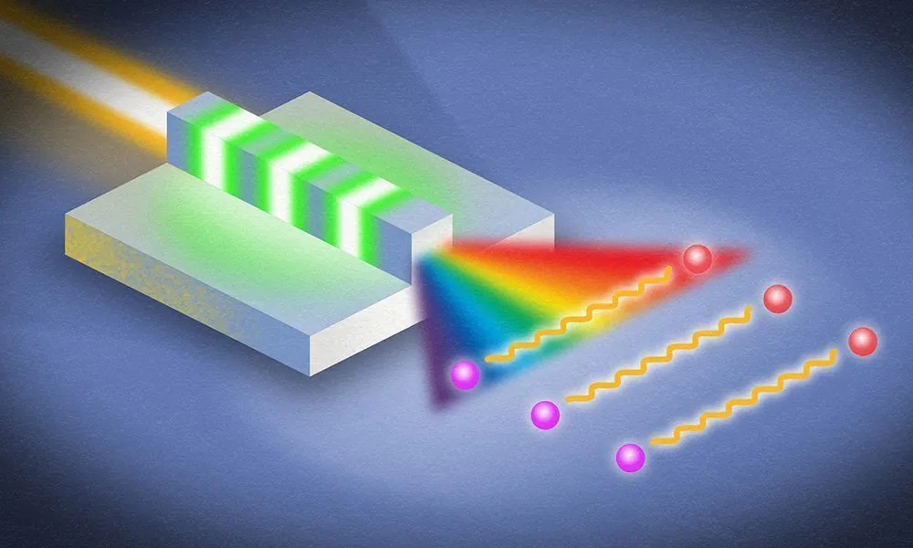
Researchers at the University of Rochester have harnessed quantum entanglement to achieve incredibly large bandwidth. They did this by using a thin-film nanophotonic device.
This new approach could lead to enhanced sensitivity and resolution for experiments in metrology and sensing, as well as higher dimensional encoding of information in quantum networks for information processing and communications.
The research was published in Physical Review Letters.
Quantum Entanglement
Quantum entanglement takes place when two quantum particles are connected to each other, and this can happen even when they are extremely far from one another. An observation of one particle affects the other, demonstrating how they are communicating with each other.
Whenever photons enter the picture and become involved in the entanglement, there are many more possibilities. For example, the photons’ frequencies can be entangled and the bandwidth can be controlled.
Qiang Lin is professor of electrical and computer engineering.
“This work represents a major leap forward in producing ultrabroadband quantum entanglement on a nanophotonic chip,” Lin says. “And it demonstrates the power of nanotechnology for developing future quantum devices for communication, computing, and sensing.”
Broadband Entanglement of Light
Current devices often rely on dividing up a bulk crystal into small sections in order to generate broadband entanglement of light. Each one of these sections slightly varies in optical properties and generates different frequencies of the photon pairs. By adding these frequencies together, a larger bandwidth can be achieved.
Usman Javid is a PhD student in Lin’s Lab and lead author of the paper.
“This is quite inefficient and comes at a cost of reduced brightness and purity of the photons,” Javid says. “There will always be a tradeoff between the bandwidth and the brightness of the generated photon pairs, and one has to make a choice between the two. We have completely circumvented this tradeoff with our dispersion engineering technique to get both: a record-high bandwidth at a record-high brightness.”
The newly developed, thin-film lithium niobate nanophotonic device created by the team relies on a single waveguide with electrodes on both sides. While a bulk device can be millimeters across, the thin-film device is extremely impressive in its 600 nanometer thickness. This makes it a million times smaller in its cross-sectional area than a bulk crystal, making the propagation of light extremely sensitive to the waveguide dimensions.
There can be major changes brought on to the phase and group velocity of the light propagating through the device just with a variation of a few nanometers. Because of this, the device allows control over the bandwidth in which the pair-generation process is momentum-matched.
“We can solve a parameter optimization problem to find the geometry that maximizes this bandwidth,” Javid says.
Deploying the Device
The team has the device ready to be deployed in experiments in a lab setting, but if it is to be used commercially, they will need to come up with a more efficient and cheaper fabrication process.
Lithium niobate fabrication is still in its infancy, and the financial aspect must be improved.
The team worked on the research alongside coauthors Jingwei Ling, Mingxiao Li, and Yang He of the Department of Electrical and Computer Engineering. The project also included Jeremy Staffa of the Institute of Optics.


