Artificial Intelligence
CDimension Launches with a Bold Mission to Rebuild the Chip Stack from the Ground Up
A new semiconductor startup, CDimension, has officially emerged from stealth with an ambitious goal: to reconstruct the foundation of computing hardware by starting at the materials level. As AI, robotics, quantum computing, and edge computing workloads grow increasingly demanding, traditional silicon architectures are running into hard limits—energy inefficiency, fragmented packaging, and bandwidth bottlenecks. CDimension is aiming to break through those barriers with a fundamentally different approach.
Reimagining the Future of Chips
At the heart of CDimension’s launch is a breakthrough in 2D semiconductor materials. Unlike conventional chips built from bulk silicon, CDimension’s process enables the direct growth of atomically thin films onto finished silicon wafers—without damaging the circuitry underneath. This innovation unlocks:
- 100× improvement in energy efficiency
- 100× boost in integration density
- 10× higher system-level speed through reduced parasitic interference
These metrics signal a dramatic leap, not just in chip performance but in what’s physically possible in modern computing design.
Solving Manufacturing’s Biggest Bottlenecks
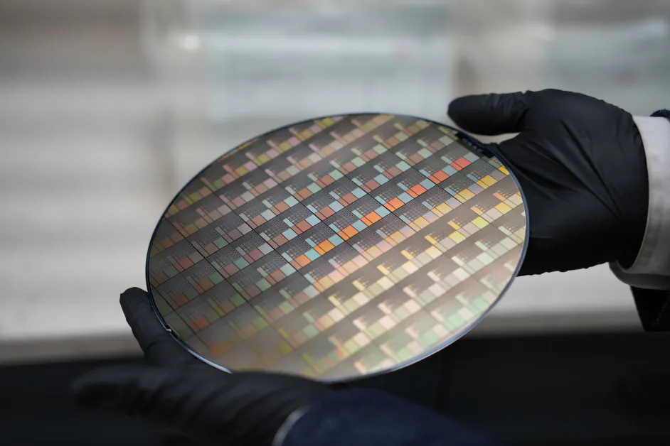
For years, 2D materials have been hailed as the next frontier for semiconductor advancement, but challenges in uniformity, scale, and integration have held them back. CDimension overcomes these barriers with a wafer-scale, low-temperature deposition process that is compatible with standard silicon manufacturing (back-end-of-line, or BEOL). The result: ultra-thin, low-leakage layers of materials like molybdenum disulfide (MoS₂), grown directly over existing silicon structures at commercial scale.
This means chipmakers can explore next-generation architectures without having to rebuild their fabs or manufacturing lines from scratch.
From Materials to Monolithic 3D Architectures
While the release of 2D materials is the company’s first commercial step, CDimension’s roadmap goes much further. Its long-term vision involves monolithic 3D chip integration—a unified structure where compute, memory, and power layers are stacked vertically using ultra-thin chiplets.
Such an architecture could redefine the future of computing by delivering:
- Compact, high-density systems
- Dramatically lower power consumption
- Localized power management for faster and more responsive systems
The company already holds multiple patents across its materials platform and architectural strategies, reinforcing its position as a deep-tech pioneer rather than a niche materials vendor.
The Team Behind the Vision
CDimension was founded by Jiadi Zhu, a Ph.D. in electrical engineering from MIT with deep expertise in energy-efficient chip design. He’s joined by Professor Tomás Palacios, one of the world’s leading experts in advanced electronic materials, who serves as a strategic advisor. Together, they bring academic rigor and commercial ambition to a problem the entire industry is struggling to solve.
Zhu stated, “We’re no longer limited by architecture alone—we’re constrained by the physical materials. To make progress, we need to rethink the entire chip stack. That starts by re-engineering what it’s made of.”
Available Now for Early Partners
CDimension’s materials are now available for commercial sampling and integration, and early adopters from both academia and industry are already evaluating them. The company offers a Premier Membership program that provides custom services, such as monolayer deposition over 3D structures and substrates up to 12 inches, supporting prototyping and design exploration.
By making this technology accessible today, CDimension is inviting forward-thinking hardware teams to co-develop the next generation of chips—ones that are no longer bound by the limitations of the past.
Implications for the Future of Computing
As the limits of traditional silicon architectures become increasingly evident, CDimension’s work signals a broader shift in how the tech industry might tackle performance, efficiency, and scalability. Instead of optimizing within the constraints of existing materials, this approach suggests a path forward where materials science and chip architecture co-evolve.
The use of atomically thin materials and monolithic 3D integration opens the door to systems that are not only more compact and energy efficient but fundamentally restructured. If widely adopted, this could lead to:
- The breakdown of current chip modularity constraints
- More localized computing architectures for edge and AI workloads
- A rethinking of power delivery and thermal management in chip design
This isn’t just a step forward for semiconductor manufacturing—it’s a redefinition of what’s possible at the intersection of materials and machine intelligence.